
Imaging - The New Frontier?
Eric Betzig
Eric Betzig is one of the Nobel laureates in chemistry in 2014 for his contribution to development of super-resolution fluorescence microscopy. His current profile says he is a group leader at Janelia, but that only tells half of the story. Betzing was trained in physics and worked at Bell labs in early 90s. Then he got fed up with academics and took a long ten year break to build the now famous microscope in his father’s garage. Of course, when he was successful, Janelia (HHMI) hired him to lead a group.
Tiring of academia, I then served as VP of R&D; in my father’s machine tool company, developing a high speed motion control technology based on an electrohydraulic hybrid drive with adaptive control algorithms. Commercial failure of the technology left me unemployed and looking for new directions. This search eventually culminated in the invention and demonstration of the superresolution technique PALM by myself and my fellow unemployed colleague and Bell Labs expatriate, Harald Hess. This story is recounted here.
-—————————————————
Gene Myers
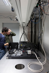
Far away in Dresden, legendary computational scientist Gene Myers is building another high-resolution microscope in his optics lab. Myers was previously at Janelia and moved to Dresden last year. Here is an interesting bio of Myers and what he is trying to achieve. Apparently his school reports say that he never liked math and was destined to be an artist.
The term friendship crops up regularly in the course of our conversation the legacy, perhaps of a childhood on the move. Born in Boise, Idaho, he soon found himself travelling far and wide. His father was an employee of oil giant Exxon and worked in various countries in Asia. The family his mother, who was French by birth, an older sister and younger brother always accompanied him.
Describing an adventurous childhood spent in Pakistan, India, Indonesia, Hong Kong and Japan, he says, I celebrated my first birthday onboard ship on the way to Karachi, and my brother was born in India. We never stayed longer than two or three years in one place. It was hard to keep leaving friends behind. On the other hand, he acquired insights into various cultures and ways of life, and learned to adapt to new circumstances.
The familys middle child began at a very early age to show a marked predilection for figures. Barely had he learned to count at the age of four, than he started to write down all the numbers from 1 to 1000. However, little Genes talent at first went unrecognized. According to my school reports, I had a gift for art. Theres no mention of mathematics.
Mathematics was his favorite subject, but he also developed a broad interest in the sciences. I read all sorts of things, like the biochemist and science fiction author Isaac Asimov, he recalls as he stirs his second cappuccino. Grays Anatomy, the standard work in anatomy, also made a huge impression on him. At twelve, he knew that he wanted to be a researcher.
-—————————————————
Jonathan Rothberg
For several months, famous scientist/entrepreneur Jonathan Rothberg has been talking about his secret new project, and the earliest information on what it is going to be came out yesterday. As it appears, Rothberg is also looking into microscopy - with an added twist.
Rothberg Returns With Star Trek-Like Medical Device To Create Images And Cut With Sound Waves
Rothberg, one of the most colorful entrepreneurs in biotech, went strangely quiet for eighteen months. Now hes back with a new incubator (called 4Combinator) and a new startup, Butterfly Network, into which he has put $20 million of his own money and $80 million more from investors to develop a device that sounds like its right out of Star Trek: an ultrasound scanner that can give vivid images quickly and cheaply, and that will eventually be able to use beams of concentrated sound to perform some types of surgical procedures.
That sounds quite revolutionary !
Also check -
With $100 Million, Entrepreneur Sees Path to Disrupt Medical Imaging
-—————————————————
There is another developing frontier of microscopy and that is with the DIY community. STM (scanning tunneling microscope) and AFM (atomic force microscope) craze started, when we were graduate students in physics. Those two technologies were supposed to allow people see things at the atomic scale through inexpensive methods. Then the microscope builders came in and turned the technology into million dollar machines by adding various anti-vibration layers. Now the DIY community has got involved to take STM and AFM to their roots.
DIY AFM
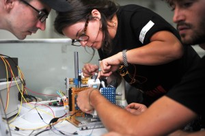
UCL students build low-cost, Arduino-powered, Lego atomic force microscope
When Alice Pyne starts talking about giving “crystallised virus structures” to school children, my heart skips a beat. Surely we’ve screwed up the next generation enough already without giving them the means to wage biological warfare.
The virus in question, the tobacco mosaic virus, “cannot infect animals,” she reassures me later. Her point is that instead of relying on 2D images in textbooks, we should be giving school children something real. Moreover, she wants them to be able to see these tiny structures in 3D with their own eyes.
Pyne, a PhD student at University College London, is trying to give schools cheap access to the expensive imaging capabilities that allowed her team to capture the first in-water image of the DNA helix structure.
And to do that, she and her colleagues are developing a 300 open-source atomic force microscope (AFM) that uses 3D-printed parts, Arduino computers and Lego bricks.
Microscope built from Lego and printed components and running on Arduino? That seems revolutionary as well !!
The microscope they constructed is built upon a metal base, with housings built from Lego and the various component holders 3D-printed to ensure a perfect fit between the Lego to the component. The scanning stage is inspired by research from Bristol University and is also 3D-printed.
Also check -
Grad students build nanometer-resolution atomic force microscope using Lego and 3D printing
-—————————————————
DIY STM
A Homemade, Open-Source Scanning Tunneling Electron Microscope
Imagine being able to examine anything you want, at the atomic level, in your living room. If Sacha De’Angeli gets his way, a scanning tunneling electron microscope – currently just the domain of research labs – will be something you can order off the Web, as an easy-to-assemble, open-source kit, for about $1000.
Scanning tunneling electron microscopes – or STMs, for short – are sophisticated imaging tools used in nanoscience and nanotechnology. The heart of the device is a conductive tip, which is guided over the surface to be observed, at a very tiny distance. An applied voltage means that a current flows between the tip and the surface, and the variation of the current reveals clues about the structure of the surface. A computer hooked to the STM processes the data, generating an image of the sample.
De’Angeli, a 34-year-old tinkerer living in Chicago who runs a website called Chemhacker, came up with the idea for the open-source STM while experimenting with creating nanoparticles in his house. He began building the STM in October, at his home and at a nearby hack space called Pumping Station: One, with the assistance of his friends Jordan Bunker and Tim Saylor. “I was trying to make a ferrofluid, and I sort of built a cool recipe to do it, but I wasn’t exactly sure if I made the actual nanoparticles,” De’Angeli says. “You can’t tell what they look like without an electron microscope. Obviously a $30,000 machine isn’t something I can afford for a hobby. I found these projects where people had built scanning tunneling electron microscopes for really not very much money. I started this project I found, that dates back to 2003 by John Alexander, and I started to modernize it a bit.”
Also check -
Building the first Open Source (inexpensive) Scanning-Tunneling Electron Microscope (STM)